

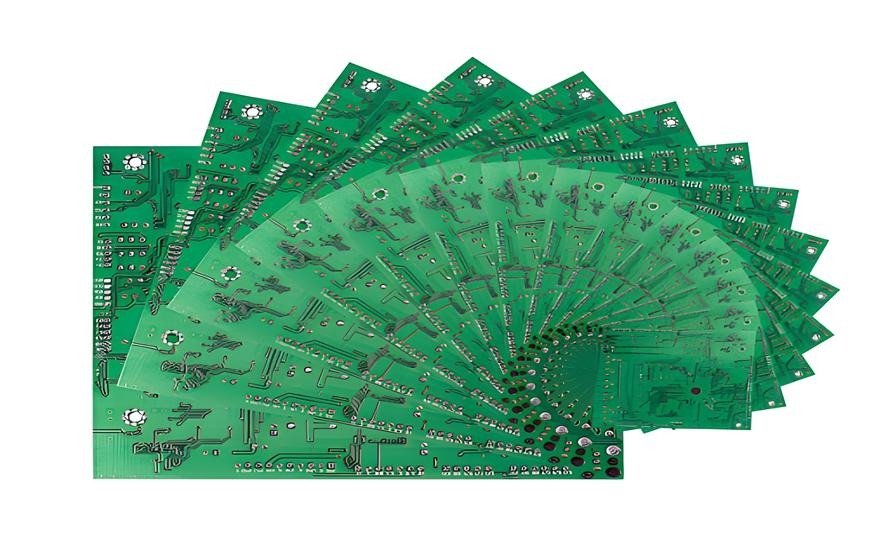
Printed circuit boards form the backbone of nearly every electronic device, providing the electrical connections and mechanical support needed for components to function efficiently. As electronic products have become more compact and feature-rich, the demand for circuit boards with greater routing capacity has increased significantly. While single-sided PCBs remain suitable for simple applications, many modern products require additional circuit density without the complexity or cost of multilayer boards. This has made the Double Sided PCB one of the most widely used PCB types across numerous industries.
A double sided PCB features conductive copper layers on both sides of the substrate, allowing electronic components and circuit traces to be placed on each surface. This design provides greater routing flexibility, supports higher component density, and enables more complex circuit designs while remaining cost-effective. Because of its versatility, double sided PCB technology is commonly found in automotive electronics, industrial control systems, consumer electronics, medical devices, power supplies, and communication equipment.
Although the design is less complex than multilayer PCBs, manufacturing a high-quality double sided board still requires precision fabrication, accurate drilling, reliable copper plating, and strict quality control. Working with an experienced Double Sided PCB manufacturer helps ensure consistent quality, dependable electrical performance, and long-term product reliability.
This article explores double sided PCB technology, its manufacturing process, advantages, applications, and why choosing the right manufacturing partner is essential.
What Is a Double Sided PCB?
A Double Sided PCB is a printed circuit board that contains conductive copper layers on both the top and bottom surfaces of the insulating substrate. Unlike a single-sided PCB, which only supports circuit traces on one side, a double sided PCB allows components and electrical connections to be placed on both sides of the board.
Electrical connections between the two copper layers are created using plated through holes, commonly known as vias. These vias enable signals and power to travel between the upper and lower layers, significantly increasing routing flexibility without requiring additional internal layers.
Double sided PCBs are typically manufactured using FR-4 fiberglass, aluminum, metal-core, or other specialized substrate materials depending on the application’s thermal, mechanical, and electrical requirements.
Their combination of design flexibility and manufacturing efficiency makes them one of the most popular PCB solutions for medium-complexity electronic products.
Why Double Sided PCBs Are Widely Used
Electronic devices continue to shrink in size while incorporating more functions and components. Single-sided circuit boards often lack sufficient routing space for these increasingly sophisticated designs.
A double sided PCB effectively doubles the available routing area by utilizing both surfaces of the board. This enables engineers to create more compact circuit layouts without significantly increasing manufacturing costs.
Using both sides of the PCB also improves component placement flexibility, allowing designers to optimize signal routing, reduce trace lengths, and enhance overall electrical performance.
Compared with multilayer PCBs, double sided boards provide an excellent balance between functionality and affordability, making them ideal for products that require moderate circuit complexity.
These advantages have made double sided PCB technology a standard choice across many commercial and industrial applications.
The Double Sided PCB Manufacturing Process
Manufacturing a double sided PCB begins with reviewing the PCB design files to ensure they meet production requirements. Engineers verify trace widths, spacing, drill sizes, via placement, and overall manufacturability before fabrication starts.
Copper-clad laminate panels are prepared before photolithography transfers the circuit patterns onto both sides of the board. Chemical etching removes unwanted copper, leaving only the required electrical circuitry.
Precision drilling equipment creates holes for component leads and plated vias. These holes are then copper plated to establish reliable electrical connections between the two sides of the PCB.
Following drilling and plating, solder mask is applied to protect the copper circuitry while leaving designated soldering areas exposed. Silkscreen printing adds component markings, reference designators, and identification information before the chosen surface finish is applied.
Finally, each completed board undergoes visual inspection, automated optical inspection, and electrical testing to verify that it meets customer specifications before shipment.
Advantages of Double Sided PCB Technology
One of the primary advantages of a double sided PCB is its increased circuit density compared to single-sided boards. Designers can utilize both surfaces for component placement and signal routing, allowing more functionality within the same board dimensions.
The additional routing flexibility also helps reduce trace congestion, improving circuit organization and simplifying complex layouts.
Electrical performance benefits from shorter signal paths and more efficient routing, while plated vias provide reliable interconnection between the two circuit layers.
Double sided PCBs are also highly cost-effective. They offer significantly greater design capability than single-sided boards while remaining less expensive than multilayer PCB solutions.
Another advantage is their compatibility with both through-hole and surface-mount assembly processes, allowing manufacturers to accommodate a wide variety of electronic components and production requirements.
These characteristics make double sided PCBs suitable for both prototype development and high-volume manufacturing.
Applications of Double Sided PCBs
Double sided PCBs are widely used across numerous industries because they provide the flexibility required for medium-complexity electronic systems. Consumer electronics manufacturers incorporate them into televisions, audio equipment, printers, home appliances, gaming devices, and smart home products.
Automotive electronics frequently utilize double sided PCBs in engine control modules, lighting systems, dashboard electronics, power management units, and vehicle sensors where reliability is essential.
Industrial automation equipment also depends on double sided circuit boards for programmable logic controllers, motor drives, industrial sensors, instrumentation, and manufacturing control systems.
Medical equipment manufacturers use double sided PCBs in patient monitoring devices, laboratory instruments, diagnostic equipment, and portable healthcare products that require compact and dependable electronic designs.
Telecommunications hardware, security systems, power supplies, LED lighting products, embedded control systems, and commercial electronics further demonstrate the versatility of double sided PCB technology.
Why Choosing an Experienced Double Sided PCB Manufacturer Matters
Although double sided PCBs are less complex than multilayer boards, precision manufacturing remains essential for achieving reliable performance. An experienced Double Sided PCB manufacturer understands the importance of accurate drilling, high-quality copper plating, precise circuit imaging, and consistent process control.
Professional manufacturers provide engineering support during product development by performing Design for Manufacturability (DFM) analysis to optimize board layouts, manufacturing tolerances, and production efficiency before fabrication begins.
Advanced manufacturing facilities equipped with automated optical inspection, CNC drilling machines, laser imaging systems, electrical testing equipment, and intelligent production management ensure consistent product quality throughout every manufacturing stage.
Working with an experienced manufacturer also helps reduce production delays, improve manufacturing yields, and ensure reliable long-term PCB performance.
Quality Assurance in Double Sided PCB Manufacturing
Quality assurance is critical throughout the manufacturing process because even minor fabrication defects can affect electrical reliability. Manufacturers inspect incoming materials before monitoring circuit imaging, etching, drilling, plating, solder mask application, and surface finishing.
Automated Optical Inspection identifies defects such as open circuits, short circuits, incorrect trace widths, and missing copper features before assembly.
Electrical testing confirms continuity, insulation resistance, and proper electrical connections between the top and bottom circuit layers. Additional inspections verify dimensional accuracy, hole positioning, solderability, and surface finish quality.
Many manufacturers also perform thermal stress testing and reliability evaluations to ensure the PCB performs consistently under real-world operating conditions.
Leading manufacturers maintain internationally recognized certifications such as ISO 9001, IPC standards, UL certification, IATF 16949 for automotive electronics, ISO 13485 for medical devices, and RoHS compliance to demonstrate their commitment to quality manufacturing.
Future Trends in Double Sided PCB Technology
Although multilayer PCBs continue to grow in popularity, double sided PCB technology remains highly relevant because of its cost-effectiveness and versatility. Advances in miniaturization, surface-mount technology, automated assembly, and precision manufacturing are allowing double sided boards to support increasingly sophisticated electronic designs.
Industries such as industrial automation, renewable energy, electric vehicles, smart appliances, and Internet of Things (IoT) devices continue driving demand for reliable medium-complexity circuit boards.
Manufacturers are investing in improved fabrication technologies, intelligent quality inspection systems, and automated production processes to enhance manufacturing precision while reducing production costs.
Conclusion
The Double Sided PCB remains one of the most practical and widely used printed circuit board solutions because it offers an excellent balance between functionality, manufacturing cost, and electrical performance. Its ability to support higher circuit density, flexible component placement, and reliable electrical connections makes it suitable for applications across consumer electronics, automotive systems, industrial automation, medical devices, telecommunications, and many other industries.
Partnering with an experienced Double Sided PCB manufacturer ensures access to advanced manufacturing technologies, engineering expertise, and comprehensive quality assurance. As electronic products continue to evolve, double sided PCB technology will remain an essential solution for building reliable, efficient, and high-quality electronic systems.